
Dow Electronic Materials
New Bump-plating Photoresist Offers Versatility and Lower Cost of Ownership
The drive in consumer demand towards smaller and thinner electronics with more functionality is well documented, as are the challenges associated with achieving integrated packages with the necessary reliability. Many packaging specialists will cite thermal management, such as changes in thermal coefficient expansion, integration of thinned wafers into stacked packages, or meeting cost targets as some of the major challenges currently facing the industry as packaging designs advance. Some of these challenges also play into changes or new material selections to better optimize current packaging designs.
Despite all of these complexities, reliability and performance of advanced semiconductor packages is often only as good as the plated structures in each package. It begins with the uniformity of plated structures across each die and across entire wafers. With the drive towards a wider variation of increasingly complex structures with denser pitches, photoresists play a critical role more than ever in wafer-level plating process steps. It is clear that focusing attention on photoresist performance can make a positive impact in the ultimate performance and reliability of the packaging, and it is also clear that packaging fabs need new options that perform well, are easy to use and are cost effective.
Currently, a majority of photoresists used for thick bump-plating applications are chemically amplified, and there are trade-offs associated with using these resists. A major disadvantage to using chemically-amplified resists in packaging fabs is the extensive environmental control that is necessary, resulting in expensive fab improvements. Resist performance issues, such as T-tops in resist profiles, can result from lack of environmental control in a fab using chemically-amplified resists. In addition, outgassing that occurs during hotplate and exposure steps can cause contamination and can obstruct venting during processing. Clearly, tight environmental control is a necessity with chemically-amplified resists. Although dry film resists can be used, chemically-amplified photoresists are typically used for bumping applications because they are easier than dry film to strip. Despite the lower initial cost of dry film, this potential savings is offset by the high cost of stripping.
In response to the need for performance, ease of use and cost effectiveness in a single resist, Dow Electronic Materials is offering INTERVIA™ BPN-65A Photoresist, a liquid, single-spin, negative-tone resist that is formulated specifically for wafer-level plating (WLP) applications. The new resist’s chemistry is an easy-to-strip formulation that uses standard 0.26N TMAH developers, avoiding the environmental control complications that come with using chemically-amplified photoresists for bump plating. Both NMP and DMSO-based strippers can work well with the resist, and the choice is dependent on the size and pitch of the features.
INTERVIA™ BPN-65A Photoresist |
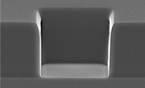 |
50 μm thickness and 25 μm via |
 |
50 μm thickness and 50 μm via |
INTERVIA™ BPN-65A Photoresist overcomes the environmental control obstacles and matches stripping capabilities while providing comparable lithographic performance to chemically-amplified resists. INTERVIA™ BPN-65A Photoresist is capable of imaging vertical sidewalls in features with 2:1 or greater aspect ratios in resist thicknesses between 30 and 60 um with excellent film thickness uniformity less than 1.5% at 1 standard deviation. INTERVIA™ BPN-65A can be use in either i-Line or broad-band exposure processing with a reduction stepper or contact aligner. In addition to a lower initial cost versus typical chemically-amplified resists, reduced cost of ownership is achieved through the low dispense volumes per wafer necessary for maximum performance of the resist. A single coat of resist is all that is needed to support thick film casting on 200 and 300 mm wafers. The dilution of this resist platform can be adjusted to fit different resist thickness requirements.
During the plating process, the photoresist exhibits no footing or undercut. INTERVIA™ BPN-65A Photoresist also has excellent chemical resistance, enabling the material to withstand a wide variety of both alkaline and acid plating chemistries as well as etching solutions. These material characteristics collectively result in plated structures with maximum integrity.
Additionally, this material provides excellent adhesion to a wide variety of metal and organic WLP substrates, including aluminum, copper, gold, nickel, titanium, silicon, silicon dioxide, glass, ceramic and polyimide. INTERVIA™ BPN-65A Photoresist retains flexibility after softbake, which is a contributing factor to the substrate compatibility of the material and to delivering improved reliability and quality.
INTERVIA™ BPN-65A Photoresist is ideal for a variety of wafer-level plating applications, including under-bump metallization (UBM), SnAg and SnPb bump plating, and Cu pillar plating. The resist is versatile enough to deliver excellent uniformity within wafer for a range of structures, such as bumps, Cu studs, capped and uncapped Cu pillars, and Cu pillar mushroom bumps.
For packaging fabs looking for a bump-plating photoresist that provides a wide range of capabilities and lower cost of ownership without the environmental control requirements inherent in chemically-amplified resists, INTERVIA™ BPN-65A Photoresist may be the ideal choice.