The commercial high volume manufacturing (HVM) of semiconductor integrated circuits (ICs) continues to evolve with new technologies to form ever-smaller transistors and other devices. In the current era, the industry has pushed the limits of miniaturization such that new materials will need to be integrated into more complex structures to continue further scaling. With an increase in the total number of materials that must be integrated into advanced device structures, the complexity of materials interactions increases rapidly and materials for chemical mechanical planarization (CMP) are no different.
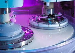
Since the CMP process must effect planar removal of one or more materials while minimizing the removal of other materials, the ability to select which materials are removed during the process is generally set by the slurry chemistry. High uniformity and low defectivity are critical to any production-worthy CMP process, of course, and those critical parameters are primarily controlled by the mechanical and structural properties of the CMP pad.
 A recent significant trend in advanced IC processing is the use of more ceria particle slurries. Originally proven for shallow-trench isolation (STI) planarization where high-selectivity of oxide to nitride is needed, ceria slurries are now being used on more layers of advanced devices. Both high-K metal gate (HKMG) structures and finFET fabrication rely on ceria slurry CMP for critical planarization needs. Different ceria slurries may be based on significantly different chemistry sets, which call for different pad properties for optimal performance. The IKONIC™ 4000 series of CMP pads from Dow Electronic Materials has been designed to provide optimal process performance when used with ceria slurries on the most challenging finFET planarization processes today.
Germanium (Ge) is just one of many new materials on the horizon that Dow is researching as part of its CMP research and development (R&D). The IC HVM industry moved to epitaxial films such as Silicon Germanium (SiGe) to build strain into devices for increased electron mobility. Now the industry is investigating pure Ge channels, and also III-V compound semiconductor channels for future transistors.
Given the vast number of materials interactions in IC fabrication, CMP R&D requires a systems perspective to comprehend the optimal combination of pad and slurry for a target application. IC fabs increasingly depend on their suppliers' understandings of the materials interactions within CMP processes to recommend the best solution for each target process.
Dow has spent decades in developing expertise regarding the planarization science of different materials, and has been working with industry leaders to integrate this expertise into manufacturing-ready solutions. Dow also works on the development of particle-free systems, which promise the ability to provide atomic-scale control.